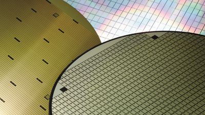
Back End Process
Achieve higher yields, enhanced traceability, and faster ROI with zero-defect quality chip production: Our combinable 2D and 3D analysis systems significantly improve quality assurance by inspecting all chips individually and evaluating the integrated circuit packaging. Integrated at the interface between the front-end and back-end, ISRA inspection systems detect defects in individual components at the wafer level and in the dicing frame. This 100% inspection ensures that only flawless material is sent to the customer.
Wafer Level Bonding
The downsizing of electronic devices is challenging semiconductor manufacturers to produce smaller component sizes while maintaining tighter process control requirements.
ISRA VISION's wafer inspection solutions for advanced wafer-level packaging ensure traceability throughout the semiconductor manufacturing process. Our systems provide superior quality control for improved device performance, enabling manufacturers to detect, resolve and monitor process deviations in a timely manner.
Benefits
- Efficiency: simultaneous scanning of the bulk wafer material, and the wafer edge
- Flexibility: seamless integration into existing process lines
- Increased uptime: minimize wafer breakage during processing
- Features
- Typical defects
- Technical data
- Reliable defect detection and classification
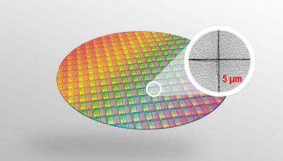
- Defect detection down to <5 µm crack width
- Wafer mapping / 2D coordination map
- Throughput: up to 180 wph
- Edge inspection tool integrated into pre-aligner
- Microcracks inside the bulk wafer material
- Edge chippings
- Cracks near edge
- Edge contaminations
- High-resolution line scan cameras with LED line illumination using different wavelengths
- Integrated adjustment of thresholds and crack characteristics for sensitive optimization of the detection result
- Typ. resolution: 20 μm, optional down to 1.5 μm
- Semi standard interface
Download additional information
 test123
CrackScan brochure en
- Filename
- brochure-crackscan-semiconductor-en.pdf
- Size
- 311 KB
- Format
 test123
CrackScan brochure cn
- Filename
- brochure-crackscan-semiconductor-cn.pdf
- Size
- 488 KB
- Format

EdgeScan brochure en
- Filename
- brochure-edgescan-semiconductor-en.pdf
- Size
- 464 KB
- Format

EdgeScan brochure cn
- Filename
- brochure-edgescan-semiconductor-cn.pdf
- Size
- 523 KB
- Format
Re-Thinning

Re-thinning can introduce defects on the wafer's surface that can impact the performance and functionality of the final semiconductor device.
Therefore, optical inspection after re-thinning is crucial to detect defects that could impact device functionality.
Conducting optical inspection after the re-thinning process allows manufacturers to minimize the risk of defects and ensure that the final semiconductor devices meet the required performance and reliability standards. This helps to enhance the overall quality and yield of the semiconductor manufacturing process.
Benefits
- Efficiency: simultaneous scanning of bulk and surface at line speeds of up to 180 wafers/hour
- Flexibility: seamless integration into existing process lines
- Increased uptime: minimize wafer breakage during processing
- Customized, seamless integration into wafer handling solutions
- 100% control of the re-thinned wafer edge in parallel to other process steps - no influence on existing cycle times
- Features
- Typical defects
- Technical data
- Reliable defect detection and classification
- Defect detection down to <5 µm crack width
- Wafer mapping / 2D coordination map
- Process control of cracks/chip-outs at the re-thinned wafer edge
- Throughput: up to 180 wph
- Edge inspection tool integrated into pre-aligner
- Microcracks inside the bulk wafer material
- Edge chippings
- Cracks near edge
- Contaminations
- High-resolution line scan cameras with LED line illumination using different wavelengths
- Integrated adjustment of thresholds and crack characteristics for sensitive optimization of the detection result
- Typ. resolution for microcrack inspection: 20 μm, optional down to 1.5 μm
- Pixel resolution for edge inspection: typ. 3 μm/px
- Integration with thin wafer handling
- Semi standard interface
Download additional information

CrackScan brochure en
- Filename
- brochure-crackscan-semiconductor-en.pdf
- Size
- 311 KB
- Format
test123
CrackScan brochure cn
- Filename
- brochure-crackscan-semiconductor-cn.pdf
- Size
- 488 KB
- Format
EdgeScan brochure en
- Filename
- brochure-edgescan-semiconductor-en.pdf
- Size
- 464 KB
- Format
EdgeScan brochure cn
- Filename
- brochure-edgescan-semiconductor-cn.pdf
- Size
- 523 KB
- Format
Post-Dicing Inspection
Dicing wafers carries the risk of defects in the dicing streets. Accurate inspection of the dicing street reliably detects these defects and minimizes the scrap rate of chips and dies. The DicingScan inspection tool provides 100% wafer inspection. High-performance line scan cameras precisely detect defects such as edge chippings in the dicing streets. In addition, the tool checks the presence, position, and completeness of the dicing streets.
With our patented MultiView imaging technology, which forms the basis of the WafQScan process, users can also inspect the rear side of the wafer through the carrier tape (foil). DicingScan ensures that only dies/chips of impeccable quality are processed.
Benefits
- Efficiency: Multiple inspection tasks in one scan
- 100% quality control: Only high-quality dies and chips are processed
- Features
- Typical defects
- Technical data
- Dicing street inspection immediately after dicing
- (Micro-)crack inspection on dies
- Check the position, integrity, and quality of dicing strees
- Front and rear side inspection, even through the carrier tape
- Uncompleted dicing
- Cracks
- Bubbles
- Releases
- Chip-outs
- MultiView technology with simultaneous image capturing
- Semi standard interface
Production analytics - Data-driven efficiency
The web-based production analytics platform allows you to check the system status of all production lines at a glance or analyze production data in detail. With the quality management system, you analyze historical data, monitor current inspection data in real-time, and identify future trends in your production process.
Early detection of production defects
Detect and quickly identify the cause of threshold value violations at every stage of production with live status information and automatic alerts. As a result you can quickly resolve production defects, shorten downtime, and reduce production costs.
Predictive maintenance
You can prevent potential system failures by analyzing real-time data from the sensors and monitoring systems. This allows proactive planning of maintenance, based on the actual condition of the machines, instead of following a fixed schedule. This data-driven approach saves costs through reduced downtime and increased overall productivity, as well as longer production line life.
Optimization of production
Dashboards allow you to compare production line and product data onsite or remotely, providing key insights for optimization. This enables you to make informed professional decisions along your value chain to increase the product quality as well as profitability. You can continuously track the progress of optimization measures and present them with visualized advanced reports.
Your benefits
- Time-saving multi-line overviews, one view for all quality-related information
- Minimize downtime by monitoring system health data
- Faster reaction to quality issues with quality data monitoring
- Fast elimination of production defects, reduction of production costs
- Improved maintenance for reduced downtime, higher overall productivity and longer production line life
Key Features
- Overview on production data and plant status
- Live insights from real time data
- Department oriented dashboards, customer specific adaptations are possible
- Web-based solution, no client software installation required
- Threshold monitoring and alerting
- Open to integrate relevant third-party data and export data to the customer's systems
Service solutions and individual trainings


For the efficient and future-proof operation of your production systems our highly qualified service teams support you globally in all matters. We provide the implementation, maintenance and servicing as well as the analysis and optimization of your systems.
Learn in the ISRA VISION Academy how our competent trainers always keep your employees up to date with the latest knowledge so that system operators, product engineers and quality managers become real inspection experts.